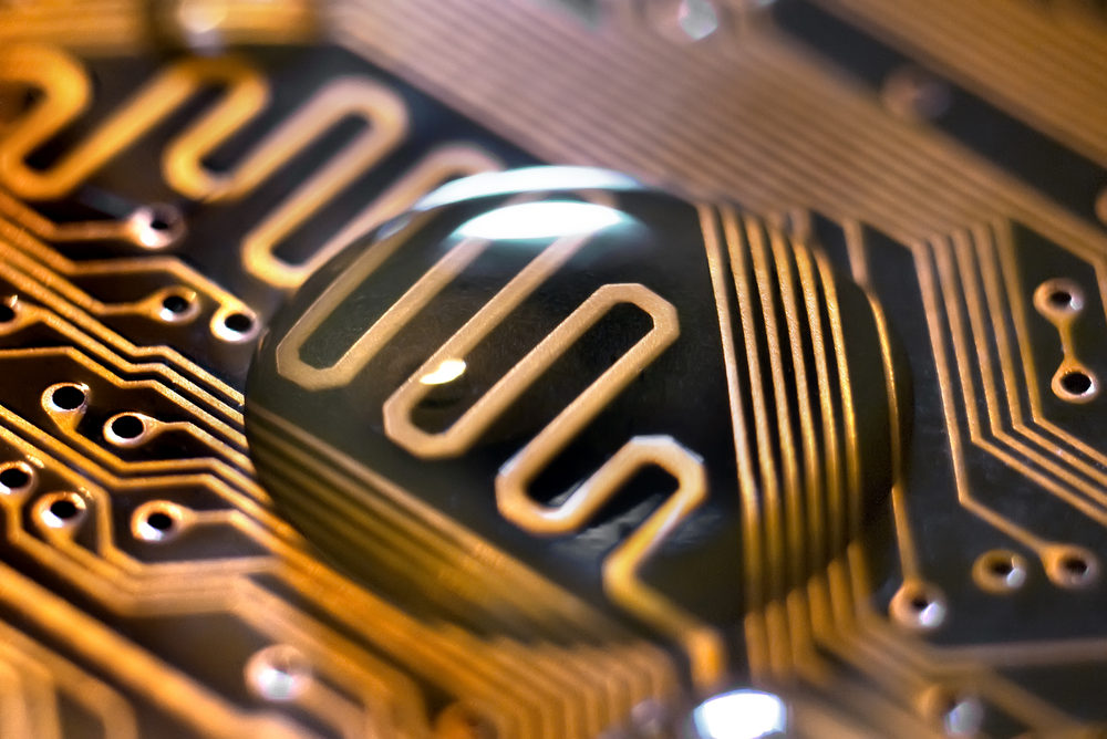
Designing a printed circuit board is not easy and there are many different aspects that must be considered. For many, a high-speed PCB layout is preferred but certain measures must be taken to ensure that this runs successfully. In this guide, we’ll talk you through high-speed PCB layout and the different things that you need to consider whilst in the design process. Keep reading to find out more.
The Schematic
Before you even begin your layout, you’ll need to draw a good schematic. Your schematic should have a steady flow to ensure that your circuit board has a natural flow in the end. Try to add as much information to your schematic as possible to ensure that everyone working on the project knows exactly what needs to be done.
When designing a high-speed PCB layout, you should also think carefully about whether you will use stripline or microstrip transmission lines. There are many benefits to both of these such as the cost-effectiveness of microstrip and the better hazard protection of stripline. Once you know what you want to use, you can go ahead and add this to your schematic.
Locations
A critical element of PCB design, especially in high-speed PCB layout is the location of the circuit components. You should also think carefully about the other components that are nearby if you want the circuit to be a success. Be clear about the exact location of the critical component’s locations and the routing paths for the signals. This will ensure that your design is perfect, and you’ll be able to reduce stress and the overall cost.
Power Supply Bypassing
If you are designing a high-speed PCB then you’ll need to think about power supply bypassing. In this element of the design, there are a few configurations that are commonly used. Rails to ground is a technique which makes use of parallel capacitors which are connected from the op amp’s pins. These are connected directly into the ground. This configuration tends to work best in most cases, so it is one to consider. The other option for high-speed PCB layout is rail to rail which makes use of bypass capacitors which are tied between the negative and the positive supply rails of the op amp. When you use rail to rail, it can offer improvements to the distortion performance and PSR.
Parasitics
No one likes when parasitics appear in your PCB and cause problems. You’ll find that they are hidden capacitors and inductors that will infiltrate your high-speed circuit. You need to make sure that you are on the lookout for these to ensure that your high-speed PCB runs smoothly. It won’t take much for your circuit performance to be affected so be vigilant.
There is a lot of things to consider when it comes to high-speed PCB layout and we have only covered the basics in this article. Take on board the advice we have given to ensure that your high-speed PCB works effectively.
- Exploring Bold Color Schemes for Your Custom Sur-Ron - January 25, 2025
- How Process Mining Tools Improve Data Collection for Better Process Visibility - January 25, 2025
- What Is the Importance of the WEE Directive? - March 15, 2024
- The Power of Enterprise Web Developers: Driving Business Success - January 29, 2024
- Why is travel nursing a viable career choice for nurse practitioners? - November 27, 2023
- Practical Tips for Boosting Fashion Store Conversions & Increasing Magento Sales - October 29, 2023
- TOP outfit ideas for women - September 12, 2023
- Ways to Effective Prevent Online Piracy in the Digital Age - August 21, 2023
- 4 Tried and Tested Tips to Make Your TikTok Videos Go Viral - July 13, 2023
- Dota 2 Player Profile: Miracle - May 11, 2023


